
If a CPU in Seoul sends a byte of information to a processor in Prague, the knowledge covers a lot of the distance as mild, zipping together with no resistance. However put each these processors on the identical motherboard, they usually’ll want to speak over energy-sapping copper, which sluggish the communication speeds attainable inside computer systems. Two Silicon Valley startups, Avicena and Ayar Labs, are doing one thing about that longstanding restrict. In the event that they succeed of their makes an attempt to lastly deliver optical fiber all the best way to the processor, it won’t simply speed up computing—it may additionally remake it.
Each firms are growing fiber-connected chiplets, small chips meant to share a high-bandwidth reference to CPUs and different data-hungry silicon in a shared package deal. They’re every ramping up manufacturing in 2023, although it could be a few years earlier than we see a pc available on the market with both product.
Ayar Labs, has succeeded at drastically miniaturizing and decreasing the facility consumption of the sorts of silicon-photonics parts used as we speak to sling bits round information facilities by means of optical-fiber cables. That gear encodes information onto a number of wavelengths of sunshine from an infrared laser and sends the sunshine by means of a fiber.
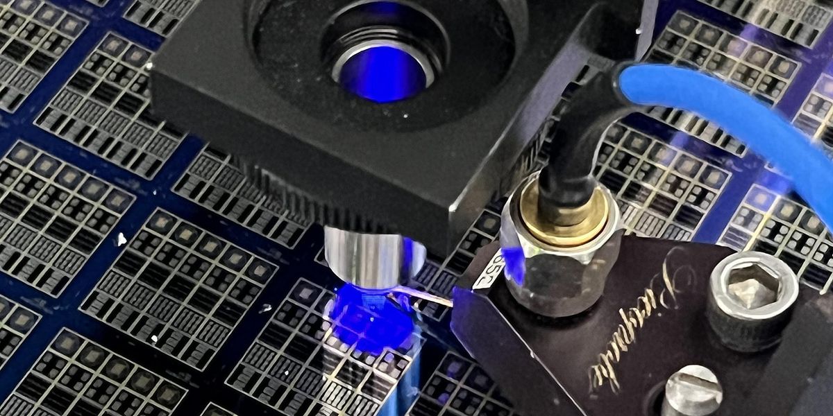
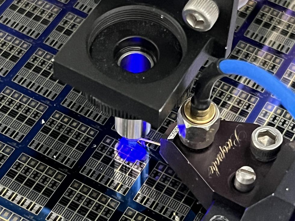
Avicena’s chiplet couldn’t be extra totally different: As a substitute of infrared laser mild, it makes use of peculiar mild from a tiny show manufactured from blue microLEDs. And as an alternative of multiplexing all of the optical information so it could journey down a single fiber, Avicena’s {hardware} sends information in parallel by means of the separate pathways in a specialised optical cable.
Ayar has the burden of historical past on its aspect, providing prospects a expertise just like what they already use to ship information over longer distances. However Avicena, the darkish horse on this race, advantages from ongoing advances within the microdisplay business, which is predicted to develop 80 p.c per 12 months and attain US $123 billion by 2030, fueled by a future filled with virtual-reality gear and even augmented-reality contact lenses.
“These firms are two ends of the spectrum by way of the chance and innovation,” says Vladimir Kozlov, founder and CEO of LightCounting, a telecommunications evaluation agency.
MicroLEDs vs. Infrared Lasers
Avicena’s silicon chiplet, LightBundle, consists of an array of gallium-nitride microLEDs, an equal-size array of photodetectors, and a few I/O circuitry to help communication with the processor it feeds with information. Twin 0.5-millimeter-diameter optical cables hyperlink the microLED array on one chiplet to the photodetectors on one other and vice versa. These cables—just like the imaging cables in some endoscopes—comprise a bundle of fiber cores that line up with the on-chip arrays, giving every microLED its personal mild path.
Apart from the existence of the sort of cable, Avicena wanted two different issues to return collectively, explains Bardia Pezeshki, the corporate’s CEO. “The primary one, which I feel was essentially the most stunning to anybody within the business, is that LEDs might be run at 10 gigabits per second,” he says. “That’s gorgeous” contemplating that the cutting-edge for visible-light communication programs simply 5 years in the past was within the a whole bunch of megahertz. However in 2021, Avicena researchers revealed a model of the microLED they dubbed cavity-reinforced optical micro-emitters, or CROMEs. The gadgets are microLEDs which have been optimized for switching pace by minimizing capacitance and sacrificing some effectivity at changing electrons to mild.
Gallium nitride isn’t one thing that’s usually built-in on silicon chips for computing, however because of advances within the microLED-display business, doing so is actually a solved drawback. In search of vivid emissive shows for AR/VR and different issues, tech giants akin to Apple, Google, and Meta have spent years developing with methods to switch already-constructed micrometer-scale LEDs to specific spots on silicon and different surfaces. Now “it’s executed by the tens of millions each day,” says Pezeshki. Avicena itself not too long ago bought the fab the place it developed the CROMEs from its Silicon Valley neighbor Nanosys.
Laptop makers will need options that won’t simply assist in the subsequent two to a few years however will give dependable enhancements for many years.
The second part was the photodetector. Silicon isn’t good at absorbing infrared mild, so the designers of silicon-photonics programs usually compensate by making photodetectors and different parts comparatively massive. However as a result of silicon readily soaks up blue mild, photodectors for Avicena’s system want solely be a couple of tenths of a micrometer deep, permitting them to be simply built-in within the chiplet below the imaging-fiber array. Pezeshki credit Stanford’s David A.B. Miller with proving, greater than a decade in the past, that blue-light-detecting CMOS photodetectors had been quick sufficient to do the job.
The mixture of imaging fiber, blue microLEDs, and silicon photodetectors results in a system that in prototypes transmits “many” terabits per second, says Pezeshki. Equally essential as the information charge is the low power wanted to maneuver a bit. “If you happen to take a look at silicon-photonics goal values, they’re a couple of picojoules per bit, and these are from firms which are manner forward of us” by way of commercialization, says Pezeshki. “We’ve already crushed these data.” In a demo, the system moved information utilizing about half a picojoule per bit. The startup’s first product, anticipated in 2023, is not going to attain all the best way to the processor however will intention to attach servers inside a data-center rack. A chiplet for chip-to-chip optical hyperlinks will observe “proper on its heels,” says Pezeshki.
However there are limits to the power of microLEDs to maneuver information. As a result of the LED mild is incoherent, it suffers from dispersion results that prohibit it to about 10 meters. Lasers, in distinction, are naturally good at going the space; Ayar’s TeraPHY chiplets have a attain of as much as 2 kilometers, probably disrupting the structure of supercomputers and information facilities much more than Avicena’s tech might. They might let pc makers utterly rethink their architectures, permitting them to assemble “primarily a single pc chip, however constructing it at rack scale,” says Ayar CEO Charlie Wuischpard. The corporate is ramping up manufacturing with its associate GlobalFoundries and is constructing prototypes with companions in 2023, although these are usually not prone to be made public, he says.
Kozlov says to anticipate many extra rivals to emerge. Laptop makers will need options that can “not simply assist in the subsequent two to a few years however will give dependable enhancements for many years.” In any case, the copper connections they’re looking for to interchange are nonetheless bettering, too.
From Your Website Articles
Associated Articles Across the Net