
The vacuum-tube triode wasn’t fairly 20 years outdated when physicists started making an attempt to create its successor, and the stakes have been big. Not solely had the triode made long-distance telephony and film sound potential, it was driving all the enterprise of economic radio, an trade value greater than a billion {dollars} in 1929. However vacuum tubes have been power-hungry and fragile. If a extra rugged, dependable, and environment friendly different to the triode could possibly be discovered, the rewards could be immense.
The objective was a three-terminal machine made out of semiconductors that will settle for a low-current sign into an enter terminal and use it to regulate the movement of a bigger present flowing between two different terminals, thereby amplifying the unique sign. The underlying precept of such a tool could be one thing referred to as the sector impact—the power of electrical fields to modulate {the electrical} conductivity of semiconductor supplies. The sector impact was already well-known in these days, due to diodes and associated analysis on semiconductors.
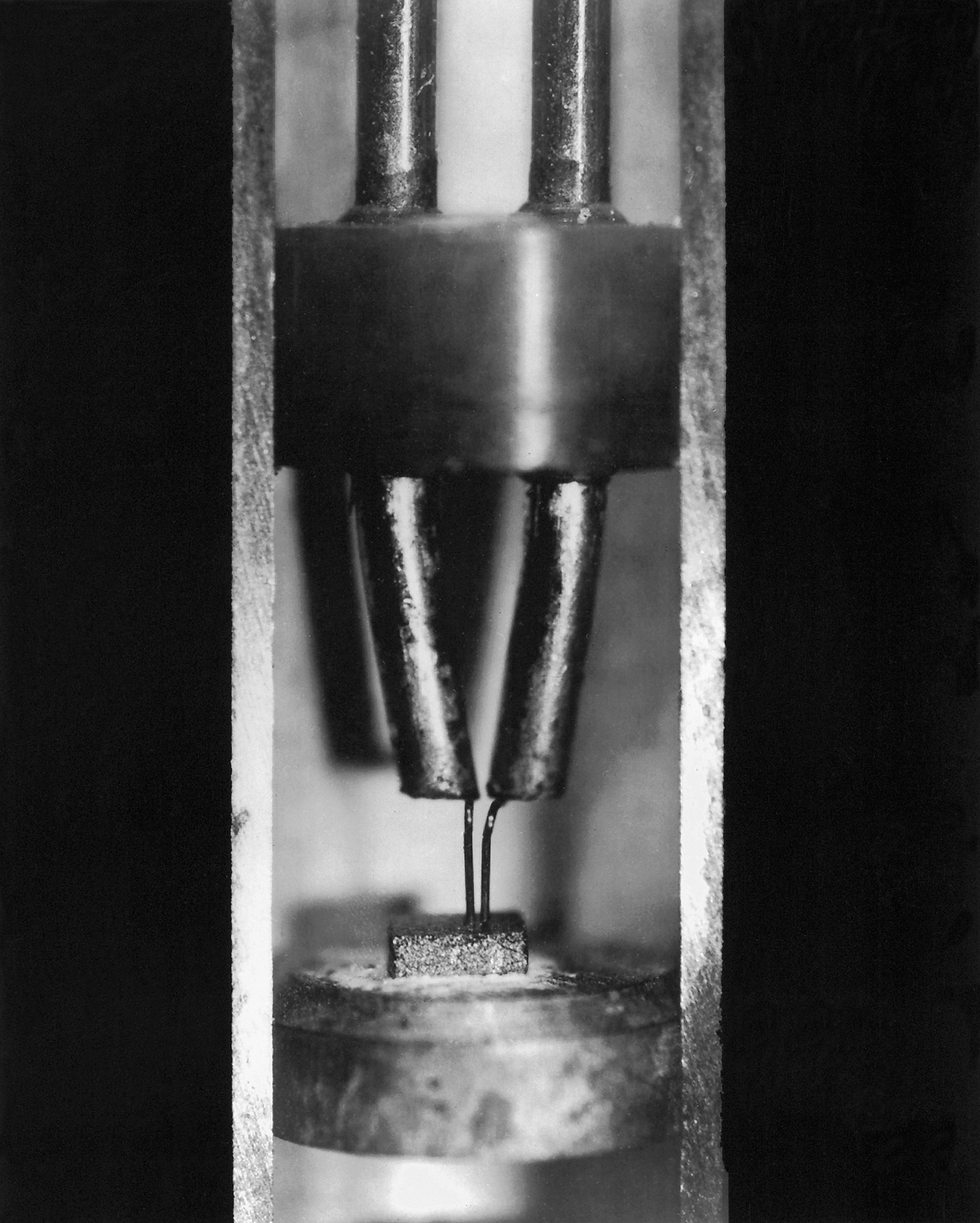 Within the cutaway photograph of a point-contact, two skinny conductors are seen; these hook up with the factors that make contact with a tiny slab of germanium. One in every of these factors is the emitter and the opposite is the collector. A 3rd contact, the bottom, is hooked up to the reverse aspect of the germanium.AT&T ARCHIVES AND HISTORY CENTER
However constructing such a tool had proved an insurmountable problem to among the world’s prime physicists for greater than 20 years. Patents for transistor-like gadgets had been filed
beginning in 1925, however the first recorded occasion of a working transistor was the legendary point-contact machine constructed at AT&T Bell Phone Laboratories within the fall of 1947.
Although the point-contact transistor was a very powerful invention of the twentieth century, there exists, surprisingly, no clear, full, and authoritative account of how the factor truly labored. Trendy, extra sturdy junction and planar transistors depend on the physics within the bulk of a semiconductor, moderately than the floor results exploited within the first transistor. And comparatively little consideration has been paid to this hole in scholarship.
It was an ungainly trying assemblage of germanium, plastic, and gold foil, all topped by a squiggly spring. Its inventors have been a soft-spoken Midwestern theoretician, John Bardeen, and a voluble and “
considerably risky” experimentalist, Walter Brattain. Each have been working underneath William Shockley, a relationship that will later show contentious. In November 1947, Bardeen and Brattain have been stymied by a easy downside. Within the germanium semiconductor they have been utilizing, a floor layer of electrons appeared to be blocking an utilized electrical discipline, stopping it from penetrating the semiconductor and modulating the movement of present. No modulation, no sign amplification.
Someday late in 1947 they hit on an answer. It featured two items of barely separated gold foil gently pushed by that squiggly spring into the floor of a small slab of germanium.
Textbooks and common accounts alike are likely to ignore the mechanism of the point-contact transistor in favor of explaining how its more moderen descendants function. Certainly, the present version of that bible of undergraduate EEs,
The Artwork of Electronics by Horowitz and Hill, makes no point out of the point-contact transistor in any respect, glossing over its existence by erroneously stating that the junction transistor was a “Nobel Prize-winning invention in 1947.” However the transistor that was invented in 1947 was the point-contact; the junction transistor was invented by Shockley in 1948.
So it appears acceptable someway that probably the most complete rationalization of the point-contact transistor is contained inside
John Bardeen’s lecture for that Nobel Prize, in 1956. Even so, studying it offers you the sense that just a few superb particulars in all probability eluded even the inventors themselves. “Lots of people have been confused by the point-contact transistor,” says Thomas Misa, former director of the Charles Babbage Institute for the Historical past of Science and Expertise, on the College of Minnesota.
Textbooks and common accounts alike are likely to ignore the mechanism of the point-contact transistor in favor of explaining how its more moderen descendants function.
A 12 months after Bardeen’s lecture, R. D. Middlebrook, a professor {of electrical} engineering at Caltech who would go on to do pioneering work in energy electronics,
wrote: “Due to the three-dimensional nature of the machine, theoretical evaluation is tough and the inner operation is, in actual fact, not but utterly understood.”
Nonetheless, and with the advantage of 75 years of semiconductor principle, right here we go. The purpose-contact transistor was constructed round a thumb-size slab of
n-type germanium, which has an extra of negatively charged electrons. This slab was handled to provide a really skinny floor layer that was p-type, which means it had an extra of constructive costs. These constructive costs are often known as holes. They’re truly localized deficiencies of electrons that transfer among the many atoms of the semiconductor very a lot as an actual particle would. An electrically grounded electrode was hooked up to the underside of this slab, creating the base of the transistor. The 2 strips of gold foil touching the floor shaped two extra electrodes, often known as the emitter and the collector.
That’s the setup. In operation, a small constructive voltage—only a fraction of a volt—is utilized to the emitter, whereas a a lot bigger unfavourable voltage—4 to 40 volts—is utilized to the collector, all with regards to the grounded base. The interface between the
p-type layer and the n-type slab created a junction identical to the one present in a diode: Primarily, the junction is a barrier that enables present to movement simply in just one path, towards decrease voltage. So present might movement from the constructive emitter throughout the barrier, whereas no present might movement throughout that barrier into the collector.
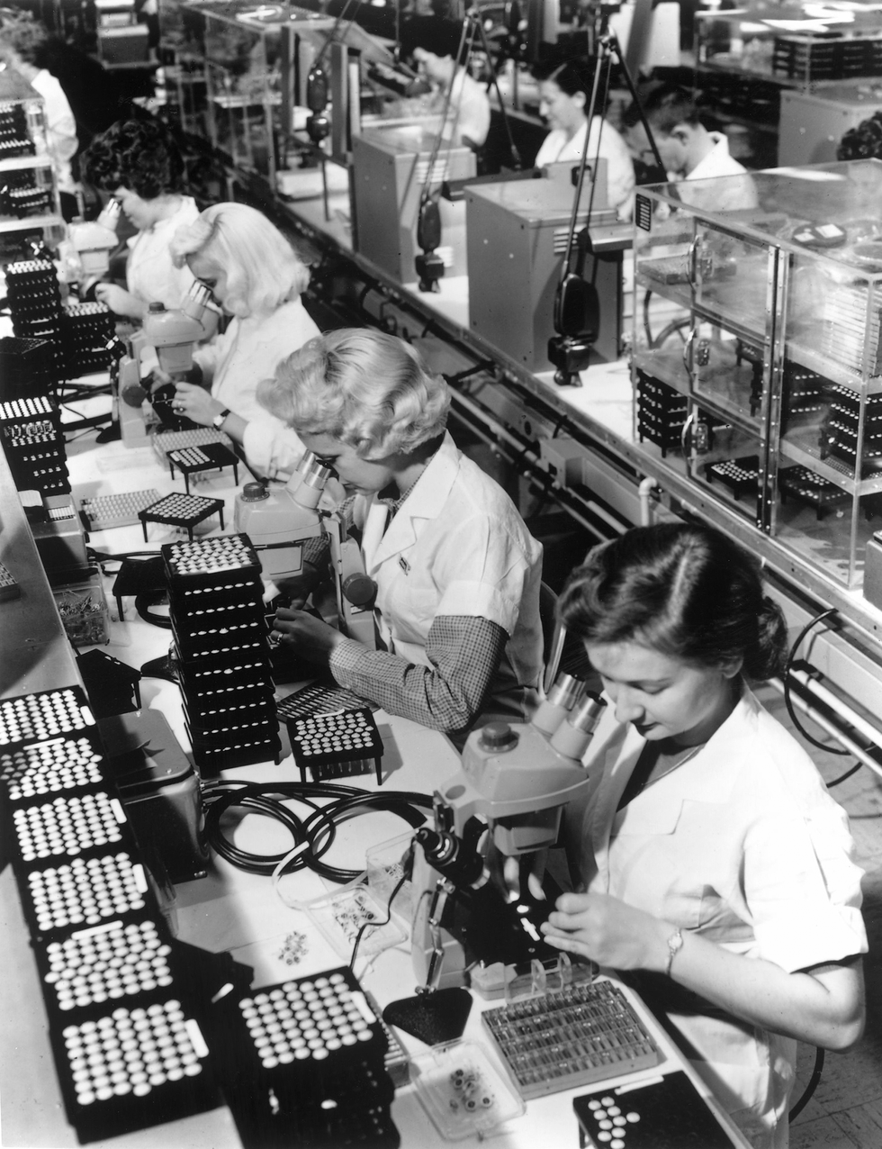 The Western Electrical Kind-2 point-contact transistor was the primary transistor to be manufactured in massive portions, in 1951, at Western Electrical’s plant in Allentown, Pa. By 1960, when this photograph was taken, the plant had switched to producing junction transistors.AT&T ARCHIVES AND HISTORY CENTER
Now, let’s take a look at what occurs down among the many atoms. First, we’ll disconnect the collector and see what occurs across the emitter with out it. The emitter injects constructive costs—holes—into the
p-type layer, and so they start transferring towards the bottom. However they don’t make a beeline towards it. The skinny layer forces them to unfold out laterally for a ways earlier than passing by the barrier into the n-type slab. Take into consideration slowly pouring a small quantity of superb powder onto the floor of water. The powder finally sinks, however first it spreads out in a tough circle.
Now we join the collector. Despite the fact that it could’t draw present by itself by the barrier of the
p–n junction, its massive unfavourable voltage and pointed form do lead to a concentrated electrical discipline that penetrates the germanium. As a result of the collector is so near the emitter, and can also be negatively charged, it begins sucking up lots of the holes which are spreading out from the emitter. This cost movement ends in a focus of holes close to the p–n barrier beneath the collector. This focus successfully lowers the “top” of the barrier that will in any other case stop present from flowing between the collector and the bottom. With the barrier lowered, present begins flowing from the bottom into the collector—rather more present than what the emitter is placing into the transistor.
The quantity of present relies on the peak of the barrier. Small decreases or will increase within the emitter’s voltage trigger the barrier to fluctuate up and down, respectively. Thus very small modifications within the the emitter present management very massive modifications on the collector, so voilà! Amplification. (EEs will discover that the capabilities of base and emitter are reversed in contrast with these in later transistors, the place the bottom, not the emitter, controls the response of the transistor.)
Ungainly and fragile although it was, it
was a semiconductor amplifier, and its progeny would change the world. And its inventors knew it. The fateful day was 16 December 1947, when Brattain hit on the concept of utilizing a plastic triangle belted by a strip of gold foil, with that tiny slit separating the emitter and collector contacts. This configuration gave dependable energy achieve, and the duo knew then that that they had succeeded. In his carpool residence that evening, Brattain informed his companions he’d simply performed “a very powerful experiment that I’d ever do in my life” and swore them to secrecy. The taciturn Bardeen, too, couldn’t resist sharing the information. As his spouse, Jane, ready dinner that evening, he reportedly stated, merely, “We found one thing right now.” With their kids scampering across the kitchen, she responded, “That’s good, expensive.”
It was a transistor, eventually, however it was fairly rickety. The inventors later hit on the concept of electrically forming the collector by passing massive currents by it throughout the transistor’s manufacturing. This system enabled them to get considerably bigger present flows that weren’t so tightly confined inside the floor layer. {The electrical} forming was a bit hit-or-miss, although. “They might simply throw out those that didn’t work,” Misa notes.
Nonetheless,
point-contact transistors went into manufacturing at many firms, underneath license to AT&T, and, in 1951, at AT&T’s personal manufacturing arm, Western Electrical. They have been utilized in listening to aids, oscillators, telephone-routing gear, in an experimental TV receiver constructed at RCA, and within the Tradic, the first airborne digital pc, amongst different methods. The truth is, point-contact transistors remained in manufacturing till 1966, partially because of their superior pace in contrast with the alternate options.
The fateful day was 16 December 1947, when Brattain hit on the concept of utilizing a plastic triangle belted by a strip of gold foil…
The Bell Labs group wasn’t alone in its profitable pursuit of a transistor. In Aulnay-sous-Bois, a suburb northeast of Paris, two German physicists, Herbert Mataré and Heinrich Welker, have been additionally making an attempt to construct a three-terminal semiconductor amplifier. Working for a French subsidiary of Westinghouse, they have been following up on very
intriguing observations Mataré had made whereas creating germanium and silicon rectifiers for the German army in 1944. The 2 succeeded in making a dependable point-contact transistor in June 1948.
They have been astounded, every week or so later, when Bell Labs lastly revealed the information of its personal transistor, at a press convention on 30 June 1948. Although they have been developed utterly independently, and in secret, the 2 gadgets have been roughly similar.
Right here the story of the transistor takes a bizarre flip, breathtaking in its brilliance and in addition disturbing in its particulars. Bardeen’s and Brattain’s boss,
William Shockley, was livid that his identify was not included with Bardeen’s and Brattain’s on the unique patent software for the transistor. He was satisfied that Bardeen and Brattain had merely spun his theories about utilizing fields in semiconductors into their working machine, and had failed to provide him adequate credit score. But in 1945, Shockley had constructed a transistor primarily based on these very theories, and it hadn’t labored.
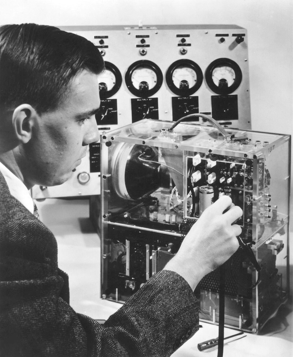 In 1953, RCA engineer Gerald Herzog led a group that designed and constructed the primary “all-transistor” tv (though, sure, it had a cathode-ray tube). The group used point-contact transistors produced by RCA underneath a license from Bell Labs. TRANSISTOR MUSEUM JERRY HERZOG ORAL HISTORY
On the finish of December, barely two weeks after the preliminary success of the point-contact transistor, Shockley traveled to Chicago for the annual assembly of the American Bodily Society. On New 12 months’s Eve, holed up in his lodge room and fueled by a potent mixture of jealousy and indignation, he started designing a transistor of his personal. In three days he scribbled
some 30 pages of notes. By the tip of the month, he had the essential design for what would grow to be often known as the bipolar junction transistor, or BJT, which might finally supersede the point-contact transistor and reign because the dominant transistor till the late Nineteen Seventies.
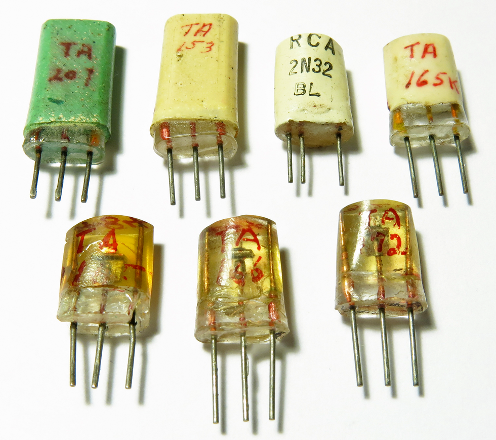 With insights gleaned from the Bell Labs work, RCA started creating its personal point-contact transistors in 1948. The group included the seven proven right here—4 of which have been utilized in RCA’s experimental, 22-transistor tv set inbuilt 1953. These 4 have been the TA153 [top row, second from left], the TA165 [top, far right], the TA156 [bottom row, middle] and the TA172 [bottom, right].TRANSISTOR MUSEUM JONATHAN HOPPE COLLECTION
The BJT was primarily based on Shockley’s conviction that costs might, and may, movement by the majority semiconductors moderately than by a skinny layer on their floor. The
machine consisted of three semiconductor layers, like a sandwich: an emitter, a base within the center, and a collector. They have been alternately doped, so there have been two variations: n-type/p-type/n-type, referred to as “NPN,” and p-type/n-type/p-type, referred to as “PNP.”
The BJT depends on primarily the identical rules because the point-contact, however it makes use of two
p–n junctions as a substitute of 1. When used as an amplifier, a constructive voltage utilized to the bottom permits a small present to movement between it and the emitter, which in flip controls a big present between the collector and emitter.
Take into account an NPN machine. The bottom is
p-type, so it has extra holes. However it is vitally skinny and frivolously doped, so there are comparatively few holes. A tiny fraction of the electrons flowing in combines with these holes and are faraway from circulation, whereas the overwhelming majority (greater than 97 %) of electrons hold flowing by the skinny base and into the collector, organising a robust present movement.
However these few electrons that do mix with holes should be drained from the bottom so as to preserve the
p-type nature of the bottom and the robust movement of present by it. That removing of the “trapped” electrons is achieved by a comparatively small movement of present by the bottom. That trickle of present allows the a lot stronger movement of present into the collector, after which out of the collector and into the collector circuit. So, in impact, the small base present is controlling the bigger collector circuit.
Electrical fields come into play, however they don’t modulate the present movement, which the early theoreticians thought must occur for such a tool to perform. Right here’s the gist: Each of the
p–n junctions in a BJT are straddled by depletion areas, by which electrons and holes mix and there are comparatively few cell cost carriers. Voltage utilized throughout the junctions units up electrical fields at every, which push costs throughout these areas. These fields allow electrons to movement all the way in which from the emitter, throughout the bottom, and into the collector.
Within the BJT, “the utilized electrical fields have an effect on the service density, however as a result of that impact is exponential, it solely takes slightly bit to create numerous diffusion present,” explains Ioannis “John” Kymissis, chair of the division {of electrical} engineering at Columbia College.
The BJT was extra rugged and dependable than the point-contact transistor, and people options primed it for greatness. However it took some time for that to grow to be apparent. The BJT was the know-how used to make built-in circuits, from the primary ones within the early Sixties all the way in which till the late Nineteen Seventies, when metal-oxide-semiconductor field-effect transistors (MOSFETs) took over. The truth is, it was these field-effect transistors, first the junction field-effect transistor after which MOSFETs, that lastly realized the decades-old dream of a three-terminal semiconductor machine whose operation was primarily based on the sector impact—Shockley’s authentic ambition.
Such a wonderful future might scarcely be imagined within the early Fifties, when AT&T and others have been struggling to provide you with sensible and environment friendly methods to fabricate the brand new BJTs. Shockley himself went on to actually put the silicon into Silicon Valley. He moved to Palo Alto and in 1956 based an organization that led the swap from germanium to silicon because the digital semiconductor of selection. Workers from his firm would go on to discovered Fairchild Semiconductor, after which Intel.
Later in his life, after dropping his firm due to his horrible administration, he grew to become a professor at Stanford and started promulgating ungrounded and unhinged theories about race, genetics, and intelligence. In 1951 Bardeen left Bell Labs to grow to be a professor on the College of Illinois at Urbana-Champaign, the place he gained a second Nobel Prize for physics, for a principle of superconductivity. (He’s the one particular person to have gained two Nobel Prizes in physics.) Brattain stayed at Bell Labs till 1967, when he joined the college at Whitman Faculty, in Walla Walla, Wash.
Shockley died a largely friendless pariah in 1989. However his transistor would change the world, although it was nonetheless not clear as late as 1953 that the BJT could be the long run. In an interview that 12 months,
Donald G. Fink, who would go on to assist set up the IEEE a decade later, mused, “Is it a pimpled adolescent, now awkward, however promising future vigor? Or has it arrived at maturity, stuffed with languor, surrounded by disappointments?”
It was the previous, and all of our lives are a lot the higher due to it.
This text seems within the December 2022 print challenge as “The First Transistor and The way it Labored .”
From Your Web site Articles
Associated Articles Across the Internet