


This can be a visitor submit in recognition of the seventy fifth anniversary of the invention of the transistor. It’s tailored from an essay within the July 2022 IEEE Electron System Society E-newsletter. The views expressed listed here are solely these of the creator and don’t characterize positions of IEEE Spectrum or the IEEE.
On the seventy fifth anniversary of the invention of the transistor, a tool to which I’ve devoted my total profession, I’d wish to reply two questions: Does the world want higher transistors? And in that case, what’s going to they be like?
I’d argue, that sure, we’re going to want new transistors, and I believe we now have some hints at present of what they are going to be like. Whether or not we’ll have the desire and financial capacity to make them is the query.
I consider the transistor is and can stay key to grappling with the impacts of world warming. With its potential for societal, financial, and private upheaval, local weather change requires instruments that give us people orders-of-magnitude extra functionality.
Semiconductors can elevate the talents of humanity like no different expertise. Virtually by definition, all applied sciences enhance human talents. However for many of them, pure sources and power constrains make orders-of magnitude enhancements questionable. Transistor-enabled expertise is a novel exception for the next causes.
- As transistors enhance, they permit new talents equivalent to computing and high-speed communication, the Web, smartphones, reminiscence and storage, robotics, synthetic intelligence, and different issues nobody has considered but.
- These talents have vast purposes, they usually remodel all applied sciences, industries, and sciences.
a. Semiconductor expertise is just not practically as restricted in progress by its materials and power usages as different applied sciences. ICs use comparatively small quantities of supplies. In consequence, they’re being made smaller, and the much less supplies they use, the quicker, extra power environment friendly, and succesful they turn out to be. - Theoretically, the power required for data processing can nonetheless be lowered to lower than one-thousandth of what’s required at present . Though we don’t but know precisely the best way to strategy such theoretical effectivity, we all know that rising power effectivity a thousandfold wouldn’t violate bodily legal guidelines. In distinction, the power efficiencies of most different applied sciences, equivalent to motors and lighting, are already at 30 to 80 p.c of their theoretical limits.
Transistors: previous, current, and future
How we’ll proceed to enhance transistor expertise is comparatively clear within the brief time period, but it surely will get murkier the farther out you go from at present. Within the close to time period, you’ll be able to glimpse the transistor’s future by taking a look at its latest previous.
The essential planar (2D) MOSFET construction remained unchanged from 1960 till round 2010, when it grew to become unattainable to additional enhance transistor density and reduce the system’s energy consumption. My lab on the College of California, Berkeley, noticed that time coming greater than a decade earlier. We reported the invention of the FinFET, the planar transistor’s successor, in 1999. FinFET, the primary 3D MOSFET, modified the flat and vast transistor construction to a tall and slim one. The profit is healthier efficiency in a smaller footprint, very similar to the good thing about multistory buildings over single-story ones in a crowded metropolis.
The FinFET can be what’s known as a thin-body MOSFET, an idea that continues to information the event of recent units. It arose from the perception that present won’t leak via a transistor inside a number of nanometers of the silicon floor as a result of the floor potential there’s nicely managed by the gate voltage. FinFETs take this thin-body idea to coronary heart. The system’s physique is the vertical silicon fin, which is roofed by oxide insulator and gate steel, leaving no silicon exterior the vary of robust gate management. FinFETs lowered leakage present by orders of magnitude and lowered transistor working voltage. It additionally pointed towards the trail for additional enchancment: decreasing the physique thickness much more.
The fin of the FinFET has turn out to be thinner and taller with every new expertise node. However this progress has now turn out to be too tough to take care of. So business is adopting a brand new 3D thin-body CMOS construction, known as gate-all-around (GAA). Right here, a stack of ribbons of semiconductor make up the skinny physique.
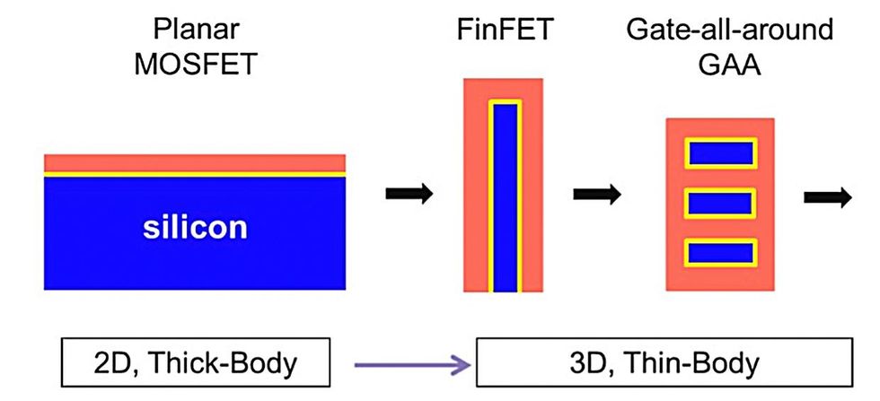
Every evolution of the MOSFET construction has been geared toward producing higher management over cost within the silicon by the gate [pink]. Dielectric [yellow] prevents cost from shifting from the gate into the silicon physique [blue].
The 3D thin-body pattern will proceed from these 3D transistors to 3D-stacked transistors, 3D monolithic circuits, and multichip packaging. In some instances, this 3D pattern has already reached nice heights. For example, the regularity of the charge-trap memory-transistor array allowed NAND flash reminiscence to be the primary IC to transition from 2D circuits to 3D circuits. Because the first report of 3D NAND by Toshiba in 2007, the variety of stacked layers has grown from 4 to past 200.
Monolithic 3D logic ICs will seemingly begin modestly, with stacking the 2 transistors of a CMOS inverter to cut back all logic gates’ footprints [see “3D-Stacked CMOS Takes Moore’s Law to New Heights”]. However the variety of stacks could develop. Different paths to 3D ICs could make use of the switch or deposition of extra layers of semiconductor movies, equivalent to silicon, silicon germanium, or indium gallium arsenide onto a silicon wafer.
The skinny-body pattern may meet its final endpoint in 2D semiconductors, whose thickness is measured in atoms. Molybdenum disulfide molecules, for instance, are each naturally skinny and comparatively massive, forming a 2D semiconductor that could be not more than three atoms vast but have excellent semiconductor properties. In 2016, engineers in California and Texas used a movie of the 2D-semiconductor molecule molybdenum disulfide and a carbon nanotube to exhibit a MOSFET with a vital dimension: a gate size simply 1 nanometer throughout. Even with a gate as brief as 1 nm, the transistor leakage present was solely 10 nanoamperes per millimeter, comparable with at present’s finest manufacturing transistor.
“The progress of transistor expertise has not been even or clean.”
One can think about that within the distant future, the whole transistor could also be prefabricated as a single molecule. These prefabricated constructing blocks is perhaps dropped at their exact areas in an IC via a course of known as directed-self-assembly (DSA). To know DSA, it could be useful to recall {that a} COVID virus makes use of its spikes to search out and chemically dock itself onto a precise spot on the floor of explicit human cells. In DSA, the docking spots, the “spikes,” and the transistor cargo are all rigorously designed and manufactured. The preliminary docking spots could also be created with lithography on a substrate, however extra docking spots could also be introduced in as cargo in subsequent steps. A number of the cargo could also be eliminated by warmth or different means if they’re wanted solely throughout the fabrication course of however not within the closing product.
Moreover making transistors smaller, we’ll must preserve decreasing their energy consumption. Right here we may see an order-of-magnitude discount via using what are known as negative-capacitance field-effect transistors (NCFET). These require the insertion of a nanometer-thin layer of ferroelectric materials, equivalent to hafnium zirconium oxide, within the MOSFET’s gate stack. As a result of the ferroelectric accommodates its personal inner electrical subject, it takes much less power to modify the system on or off. A further benefit of the skinny ferroelectric is the attainable use of the ferroelectric’s capability to retailer a bit because the state of its electrical subject, thereby integrating reminiscence and computing in the identical system.
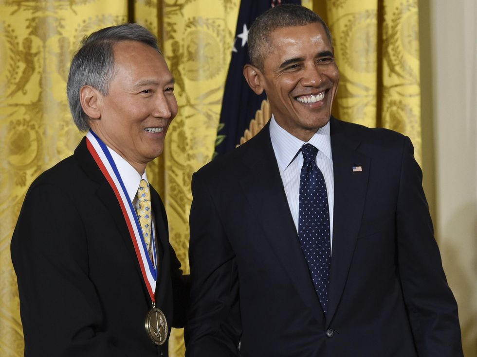
The creator [left] obtained the U.S. Nationwide Medal of Expertise and Innovation from President Barack Obama [right] in 2016.
Kevin Dietsch/UPI/Alamy
To some extent the units I’ve described arose out of current tendencies. However future transistors could have very completely different supplies, buildings, and working mechanisms from these of at present’s transistor. For instance, the nanoelectromechanical change is a return to the mechanical relays of many years previous somewhat than an extension of the transistor. Moderately than counting on the physics of semiconductors, it makes use of solely metals, dielectrics, and the power between intently spaced conductors with completely different voltages utilized to them.
All these examples have been demonstrated with experiments years in the past. Nevertheless, bringing them to manufacturing would require rather more effort and time than earlier breakthroughs in semiconductor expertise.
Attending to the long run
Will we have the ability to obtain these feats? Some classes from the previous point out that we may.
The primary lesson is that the progress of transistor expertise has not been even or clean. Round 1980, the rising energy consumption per chip reached a painful degree. The adoption of CMOS, changing NMOS and bipolar applied sciences—and later, the gradual discount of operation voltage from 5 volts to 1—gave the business 30 years of kind of simple progress. However once more, energy grew to become a problem. Between 2000 and 2010, the warmth generated per sq. centimeter of IC was projected by considerate researchers to quickly attain that of the nuclear-reactor core. The adoption of 3D thin-body FinFET and multicore processor architectures averted the disaster and ushered in one other interval of comparatively clean progress.
The historical past of transistor expertise could also be described as climbing one mountain after one other. Solely after we bought to the highest of 1 had been we ready see the vista past and map a path to climb the subsequent taller and steeper mountain.
The second lesson is that the core energy of the semiconductor business—nanofabrication—is formidable. Historical past proves that, given adequate time and financial incentives, the business has been in a position to flip any concept into actuality, so long as that concept doesn’t violate scientific legal guidelines.
However will the business have adequate time and financial incentives to proceed climbing taller and steeper mountains and preserve elevating humanity’s talents?
It’s a good query. Even because the fab business’s sources develop, the mountains of expertise improvement develop even quicker. A time could come when nobody fab firm can attain the highest of the mountain to see the trail forward. What occurs then?
The income of all semiconductor fabs (each impartial and people, like Intel, which might be built-in firms) is about one-third of the semiconductor business income. However fabs make up simply 2 p.c of the mixed revenues of the IT, telecommunications, and consumer-electronics industries that semiconductor expertise allows. But the fab business bears a lot of the rising burden of discovering, producing, and advertising new transistors and nanofabrication applied sciences. That should change.
For the business to outlive, the comparatively meager sources of the fab business should be prioritized in favor of fab constructing and shareholder wants over scientific exploration. Whereas the fab business is lengthening its analysis time horizon, it wants others to tackle the burden too. Humanity’s long-term problem-solving talents deserve focused public help. The business wants the assistance of very-long-term exploratory analysis, publicly funded, in a Bell Labs–like setting or by college researchers with career-long timelines and wider and deeper information in physics, chemistry, biology, and algorithms than company analysis at present permits. This fashion, humanity will proceed to search out new transistors and achieve the talents it might want to face the challenges within the centuries forward.
Concerning the Writer
Chenming Hu is the recipient of the 2020 IEEE Medal of Honor, the 2014 U.S. Nationwide Medal of Expertise and Innovation, and different honors. An IEEE Life Fellow, Hu led the event of the FinFET, the system utilized by most superior pc processors at present. He has been a professor on the College of California, Berkeley, since 1976.